
OCR Specification focus:
‘Account for voltmeter loading and source resistance when designing potential divider circuits.’
A potential divider is widely used in circuits to provide specific voltages or to measure sensor outputs. However, real circuits experience limitations such as loading effects and source resistance, which alter expected voltages and lead to measurement inaccuracies. Understanding and accounting for these effects is crucial when designing accurate and reliable circuits in both experimental and practical applications.
Understanding Potential Divider Limitations
A potential divider uses resistors (or variable components like thermistors and LDRs) to divide an input potential difference into smaller, controlled outputs. The voltage across each resistor depends on its resistance relative to the total resistance of the divider. Although theory predicts precise voltage outputs, practical circuits rarely behave ideally. The presence of finite internal resistance in the power source and non-infinite resistance in connected devices or meters introduces systematic errors known as loading effects.
Ideal versus Real Circuits
In ideal conditions:
The potential divider’s output voltage depends solely on resistor ratios.
The source has zero internal resistance, meaning no energy is lost internally.
The connected device (such as a voltmeter or sensor input) has infinite resistance, ensuring no current is drawn from the divider.
In reality:
The source exhibits internal resistance that reduces the available output voltage under load.
The connected device has finite resistance, drawing additional current and altering voltage distribution.
These limitations distort the output and must be considered when predicting or measuring circuit performance.
Source Resistance and Its Effect
Every power source has an internal resistance, denoted r, representing the resistance within the battery or power supply.
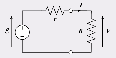
Model of a non-ideal source consisting of an ideal emf E in series with an internal resistance r, with external terminals indicated. This highlights how terminal p.d. falls under load, impacting divider outputs and measurement accuracy. The diagram is limited to exactly the elements required by the OCR specification. Source.
When current flows, part of the energy is dissipated within this resistance, reducing the terminal potential difference available to the external circuit.
EQUATION
—-----------------------------------------------------------------
Terminal Potential Difference (V) = emf (E) – Current (I) × Internal Resistance (r)
E = Electromotive force, measured in volts (V)
I = Current, measured in amperes (A)
r = Internal resistance of the source, measured in ohms (Ω)
—-----------------------------------------------------------------
When a potential divider is connected to a real source, the source resistance forms part of the total circuit resistance. This changes the current flowing and consequently affects the voltage division ratio. For example, if the load on the divider draws significant current, the voltage across the load will drop due to energy loss within the source. Therefore, when designing dividers for precision voltage outputs, internal resistance must be minimised or compensated for.
The Loading Effect Explained
The loading effect occurs when the device connected to the output of a potential divider draws current, effectively placing its resistance in parallel with one of the divider resistors.
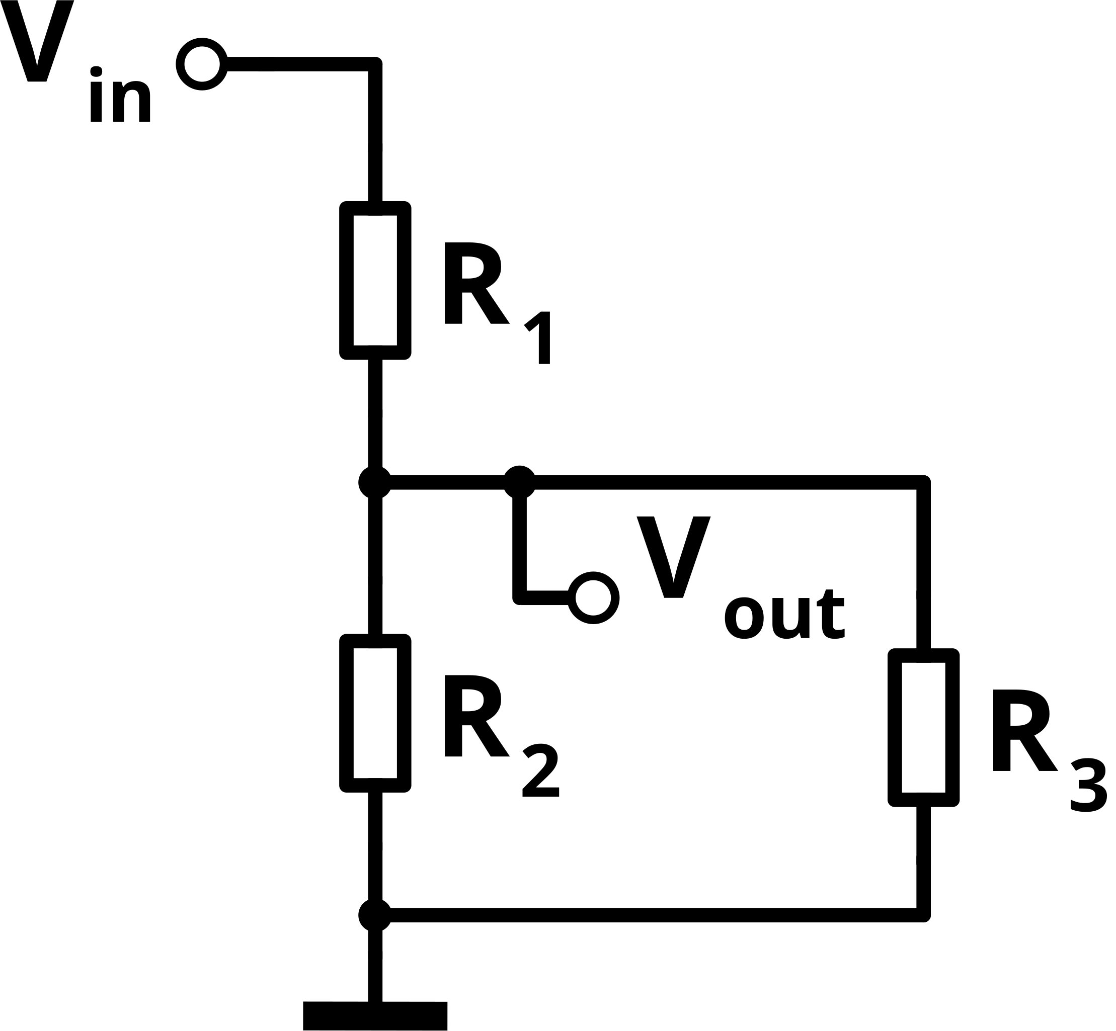
A clean schematic of a loaded potential divider, showing Rₗ connected across R₂ so the effective resistance is reduced and V_out falls below its unloaded value. Labels for R₁, R₂, Rₗ, and the output node make the parallel loading clear. This diagram contains no extra material beyond what is required for OCR A-Level study. Source.
Loading Effect: The reduction in output voltage from a potential divider caused by the finite resistance of the connected load or measuring instrument.
The voltmeter or sensor forms a parallel branch, reducing the equivalent resistance across that part of the divider. The total resistance of the divider changes, and the output voltage becomes smaller than calculated under ideal conditions. The larger the current drawn by the connected device, the greater the voltage drop due to loading.
Mathematical Representation
If a potential divider consists of resistors R₁ and R₂, the unloaded output voltage across R₂ is given by:
EQUATION
—-----------------------------------------------------------------
Output Voltage (V_out) = (R₂ / (R₁ + R₂)) × V_in
V_in = Input voltage applied across the divider (V)
R₁, R₂ = Resistor values (Ω)
—-----------------------------------------------------------------
When a load resistance R_L is connected across R₂, the effective resistance of that branch becomes:
EQUATION
—-----------------------------------------------------------------
R_effective = (R₂ × R_L) / (R₂ + R_L)
R_L = Load resistance (Ω)
—-----------------------------------------------------------------
This lowers the output voltage to a new value, calculated by replacing R₂ with R_effective in the original potential divider equation. As R_L decreases (i.e. as the device draws more current), R_effective decreases, and V_out falls further from the ideal value.
Designing to Minimise Loading Effects
To reduce loading and maintain accuracy:
Ensure R_L >> R₂, meaning the connected device’s resistance should be much greater than the lower resistor in the divider. This keeps the load current negligible and preserves the intended voltage ratio.
Use a buffer amplifier (such as an operational amplifier in voltage follower configuration) between the divider and the measuring device. A buffer has extremely high input resistance and negligible current draw, effectively isolating the divider from the load.
Choose resistor values appropriately — too high values increase susceptibility to noise and leakage, while too low values draw excessive current, wasting power and increasing internal losses.
Account for internal resistance when selecting resistor ratios. Use the measured terminal voltage rather than the emf to set accurate division ratios.
Impact on Measuring Instruments
Real voltmeters and data-logging inputs have finite input resistances, often 1 MΩ or greater for digital instruments. However, if the potential divider uses high resistance values (in the order of megaohms), even this high input resistance can cause measurable loading. Analogue meters, with much lower input resistance, produce more significant voltage drops. When designing circuits for measurement, the instrument’s input resistance must always be included in circuit analysis to predict the true output voltage.
Practical Awareness and Measurement Accuracy
In laboratory practice, students must justify their measuring techniques by recognising limitations such as loading effects and source resistance. This ensures reliable data interpretation and accurate experimental results. Allowing components to cool and avoiding excessive currents also prevent resistance changes due to temperature, which can compound measurement errors.
By incorporating realistic assumptions into circuit design and acknowledging the presence of internal and loading resistances, accurate and stable potential divider performance can be achieved in practical applications.
Practice Questions
Question 1 (2 marks)
Explain what is meant by the loading effect in a potential divider circuit and state how it affects the output voltage when a low-resistance load is connected.
Mark scheme:
1 mark for defining the loading effect: reduction in output voltage due to the finite resistance of a connected device or instrument.
1 mark for stating that a low-resistance load draws more current, reducing the potential difference across the output resistor and hence lowering the measured output voltage.
Question 2 (5 marks)
A potential divider is designed to supply a variable output voltage to a data-logger input. The divider consists of two resistors, R1 = 8.0 kΩ and R2 = 4.0 kΩ, connected across a 12 V supply. The data-logger input has a resistance of 12 kΩ and is connected across R2.
(a) Calculate the ideal output voltage of the divider before the data-logger is connected.
(b) Calculate the effective resistance across R2 when the data-logger is connected.
(c) Determine the new output voltage and comment on the effect of loading in this case.
Mark scheme:
(a) 1 mark: Recognises use of divider equation Vout = (R2 / (R1 + R2)) × Vin
→ Vout = (4.0 / (8.0 + 4.0)) × 12 = 4.0 V.(b) 2 marks:
1 mark for using parallel resistance formula R_effective = (R2 × R_load) / (R2 + R_load).
1 mark for correct calculation: R_effective = (4.0 × 12) / (4.0 + 12) = 3.0 kΩ.
(c) 2 marks:
1 mark for recalculating output voltage using new R_effective:
Vout = (3.0 / (8.0 + 3.0)) × 12 = 3.27 V.1 mark for correct comment: Output voltage is reduced from 4.0 V to 3.27 V due to loading; the data-logger’s finite resistance draws current and lowers Vout.
FAQ
Using very large resistor values reduces the current drawn from the power supply, which conserves energy but increases circuit sensitivity to loading and leakage currents.
High-value resistors also make the circuit more susceptible to noise and interference, as small stray currents can cause significant voltage changes. In precision applications, it’s better to choose moderate resistor values to balance stability with low power consumption.
A simple method is to measure the output voltage of a potential divider with and without a voltmeter or resistor connected across the output.
First, record the open-circuit voltage (no load).
Then, connect a load resistor or voltmeter and record the new voltage.
The drop in output voltage shows the loading effect caused by the finite resistance of the measuring device.
This experiment helps quantify how the load resistance alters voltage distribution.
When the load resistance is much greater than the lower resistor of the divider (R_L >> R₂), very little current flows through the load.
This means the load draws minimal current, leaving the voltage division almost unchanged from its theoretical value. Digital voltmeters and buffer amplifiers exploit this principle by having extremely high input resistances, often several megaohms or more, to minimise loading.
As temperature increases, most resistive materials experience an increase in resistance due to greater lattice vibrations impeding electron flow.
This can cause the divider’s resistor ratios to change slightly, modifying the output voltage.
Metal film resistors have low temperature coefficients and offer greater stability.
Carbon or wire-wound resistors may vary more significantly, influencing precision circuits and worsening loading-related errors.
Engineers often use voltage followers or buffer amplifiers to isolate the potential divider from the next stage of a circuit.
Other strategies include:
Selecting a divider with a low output impedance relative to the load input impedance.
Using calibration circuits to correct for predictable voltage drops.
Employing feedback systems that maintain a stable output regardless of load current.
These approaches preserve measurement accuracy and prevent sensor readings from being distorted by loading effects.
