
OCR Specification focus:
‘Diamond, graphite, graphene and silicon have giant covalent lattices. Properties and melting points across Periods 2–3 are explained by structure and bonding changes.’
Giant covalent lattices feature extensive networks of atoms joined by strong covalent bonds. Their distinct structures explain variations in physical properties and melting points across key Period-2 and Period-3 elements.
Giant Covalent Structures in Periodicity
Giant covalent lattices are vast, continuous networks of atoms connected by strong covalent bonds. These structures require significant energy to overcome, resulting in high melting points and characteristic physical behaviours across diamond, graphite, graphene and silicon. Understanding structural differences allows prediction and explanation of melting-point trends across Periods 2 and 3.
Diamond: Tetrahedral Giant Lattice
Diamond consists of carbon atoms bonded in a tetrahedral arrangement, where each carbon forms four σ-bonds with neighbouring atoms. This creates a rigid, three-dimensional giant lattice extending throughout the entire solid.
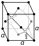
This diagram shows the diamond-cubic giant covalent lattice, where each atom is bonded tetrahedrally to four neighbours in three dimensions. The repeating unit cell illustrates how this structure extends throughout diamond and silicon, giving very high melting points. The full crystallographic unit-cell detail goes beyond OCR requirements, but the tetrahedral bonding pattern is directly relevant. Source
Tetrahedral arrangement: A molecular or lattice geometry in which a central atom is bonded to four others positioned at the corners of a tetrahedron.
The extensive strength and number of covalent bonds in diamond explain its extremely high melting point.
Key structural features of diamond
Each carbon forms four covalent bonds.
No delocalised electrons; all electrons are localised in σ-bonds.
Very rigid structure with minimal atomic movement.
High bond enthalpy throughout the lattice.
Resulting properties
Very high melting point due to many strong covalent bonds.
Hardness arising from strong, directional bonding.
Electrical insulating behaviour, as mobile charge carriers are absent.
Graphite: Layered Giant Covalent Structure
Graphite also contains carbon but differs from diamond because each carbon atom forms three covalent bonds, creating trigonal planar layers. Between these layers, weak London dispersion forces allow slippage.
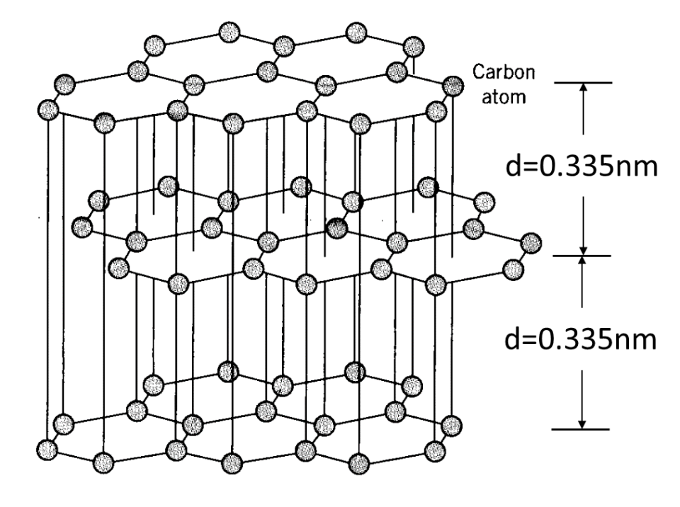
This ball-and-stick diagram shows graphite’s hexagonal carbon layers stacked in an ABAB pattern. Strong covalent bonds hold atoms together within each sheet, while weak van der Waals forces act between the layers, allowing them to slide. The labelled interlayer spacing includes structural detail beyond the OCR specification but supports the explanation of weak forces. Source
London dispersion forces: Weak intermolecular forces arising from temporary dipoles caused by electron movement.
Graphite’s mixed bonding accounts for its unusual combination of high melting point and lubrication properties.
Key structural features of graphite
Each carbon forms three σ-bonds, leaving one delocalised electron.
Layers of hexagonal carbon rings arranged in parallel sheets.
Weak forces between layers permit sliding.
Resulting properties
High melting point, as breaking the lattice requires overcoming strong covalent bonds within layers.
Electrical conductivity along layers due to delocalised electrons.
Soft, flaky texture from layer slippage.
Graphene: Single-Layer Giant Covalent Network
Graphene is a single atom-thick sheet of carbon arranged in hexagonal rings. It is essentially one isolated layer of graphite, yet with distinct mechanical and electrical behaviours.
Graphene’s structure comprises strong covalent bonds in two dimensions, resulting in exceptional strength and thermal stability.
Key structural features of graphene
One-atom-thick carbon sheet.
Each carbon forms three covalent bonds with one delocalised electron.
Continuous two-dimensional hexagonal lattice.
Resulting properties
Very high melting point because covalent bonding must be completely broken to melt the sheet.
Excellent electrical conductivity from freely mobile delocalised electrons.
High mechanical strength and elasticity.
Silicon: Giant Covalent Lattice in Period 3
Silicon forms a giant covalent lattice similar to diamond but with Si—Si covalent bonds, which are longer and weaker than C—C bonds. This accounts for silicon’s comparatively lower, yet still high, melting point.
Covalent bond: A chemical bond formed by the sharing of a pair of electrons between two atoms.
Silicon’s lattice properties reflect its position in Period 3 and the nature of larger atoms forming weaker covalent interactions.
Key structural features of silicon
Tetrahedral lattice similar to diamond.
Longer Si—Si bonds due to larger atomic radius.
Extensive network requiring significant energy to break.
Resulting properties
High melting point, though lower than diamond.
Semiconducting behaviour due to limited electron mobility.
Moderate hardness compared with carbon lattices.
Melting-Point Variations Across Periods 2 and 3
Melting-point trends across Periods 2 and 3 reflect changes in structure and bonding rather than atomic mass or simple periodic position.
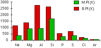
This graph shows how the melting points and boiling points of Period‑3 elements vary from sodium to argon. The metals and silicon have high melting points because of strong metallic or giant covalent lattices, while molecular elements have much lower values due to weak intermolecular forces. The inclusion of boiling‑point data extends beyond OCR requirements but reinforces the bonding explanation. Source
Factors influencing melting-point variation
Bond strength: C—C bonds are stronger than Si—Si, contributing to diamond having a higher melting point than silicon.
Dimensionality of bonding: Graphite and graphene have 2D covalent bonding but still require significant energy to disrupt.
Presence of delocalised electrons: Does not significantly lower melting point, as covalent lattice disruption dominates thermal requirements.
Melting-point comparisons
Diamond: highest due to fully three-dimensional strong bonding.
Graphite/Graphene: extremely high due to strong intralayer bonding.
Silicon: high but lower than carbon lattices because of weaker covalent bonds.
Why Structure Determines Melting Point
Melting requires converting an ordered lattice into a disordered liquid. For giant covalent lattices, this involves breaking thousands of strong covalent bonds per atom. Thus structural features directly dictate the thermal stability of these substances.
Summary points for structural influence
More extensive bonding networks increase melting point.
Stronger covalent bonds require greater thermal energy for disruption.
Variations between carbon and silicon arise from atomic radius and bond strength differences.
Practice Questions
Diamond and graphite are both forms of carbon but have very different melting points.
Explain why diamond has a much higher melting point than graphite.
(3 marks)
Diamond has a three-dimensional structure in which each carbon forms four strong covalent bonds. (1 mark)
A large amount of energy is required to break these many strong covalent bonds throughout the lattice. (1 mark)
Graphite contains layers held together by weak forces, so less energy is needed to separate the layers compared with breaking diamond’s full 3D network. (1 mark)
The melting points of silicon and carbon (in diamond form) differ significantly despite both forming giant covalent lattices.
Using your knowledge of bonding and structure, explain:
(a) the similarities in their structures,
(b) why their melting points differ, and
(c) why silicon conducts electricity differently from graphite.
(6 marks)
(a) Structural similarities
Both silicon and diamond have a tetrahedral arrangement around each atom. (1 mark)
Each atom forms four covalent bonds in a giant covalent lattice. (1 mark)
(b) Differences in melting point
Si–Si bonds are weaker than C–C bonds because silicon atoms are larger and have longer bond lengths. (1 mark)
Therefore less energy is required to break the covalent lattice in silicon, giving it a lower melting point. (1 mark)
(c) Electrical conduction
Silicon is a semiconductor because it has limited availability of charge carriers. (1 mark)
Graphite conducts electricity because each carbon atom has one delocalised electron that can move freely within the layers. (1 mark)
FAQ
The directional nature of covalent bonds means each bond is fixed in a specific orientation, creating rigid and predictable structures.
In diamond, tetrahedral bonding locks atoms firmly in place, producing exceptional hardness.
In graphite and graphene, bonding is confined to two dimensions, so the layers remain strong but can still slide due to weak forces between them.
Giant covalent lattices require breaking covalent bonds, whereas metallic lattices involve overcoming electrostatic attractions between positive ions and delocalised electrons.
Covalent bond breaking demands far more energy than distorting or separating metallic ions.
As a result, giant covalent solids remain solid at much higher temperatures.
In silicon, the energy gap between the valence band and conduction band is small enough for some electrons to move at higher temperatures.
Diamond has a much larger band gap, preventing electrons from being thermally promoted.
Therefore, silicon can conduct modestly, whereas diamond remains an electrical insulator.
In 3D lattices like diamond, vibrations travel uniformly through the structure, giving diamond extremely high thermal conductivity.
In 2D systems like graphene, heat spreads rapidly along the plane of the sheet but not perpendicular to it.
This creates highly anisotropic thermal properties.
Melting graphite requires breaking strong covalent bonds within each layer, not just separating layers.
To melt, the entire 2D covalent network must be disrupted, which requires very high energy input.
The weak forces only influence ease of sliding, not the energy needed to convert the solid to a liquid.
